I2S
To handle analog audio input and output we wanted to use a Digilent PMOD I2S2. For this we could use the Xilinx provided I2S IP, but we decided against that because it required software to function in the way we wanted and it requires a lot of area (around 1000 LUT and 3000 FF). Writing our own took this down to 100 LUT and 200 FF.
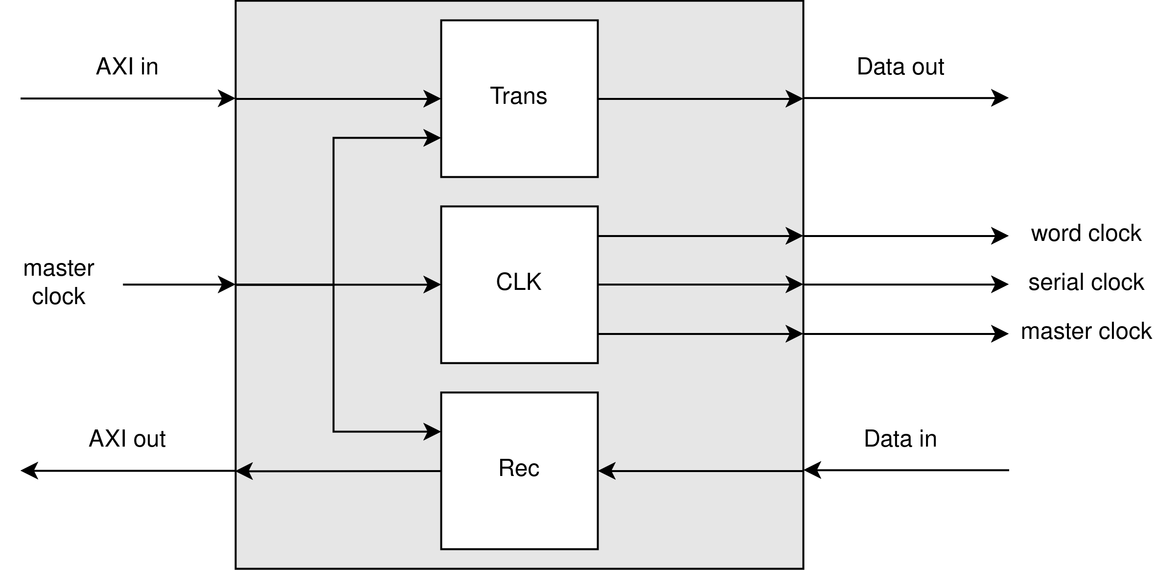
Clock generation
After some unexpected troubles with clocking, we landed on a simple design which takes in a master clock and applies two configurable clock dividers to arrive at a serial and word clock which are in sync with the master clock. This is a very simple approach which essentially just translates parameters found in the Digilent data sheets into a proper clock for our use case.
Transmitter
The transmitter takes in a master clock and our custom audio AXI standard. It is capable of generating its own word and serial clocks when working in a standalone fashion. It essentially takes the data sent to it over AXI and shift registers this in sync with the right clocks onto the data line.
Receiver
The receiver takes in a master clock and our custom audio AXI standard. It is capable of generating its own word and serial clocks when working in a standalone fashion. It essentially takes the data sent to it over the data line and shift registers it into a buffer which can be sent over AXI stream.
Wrapper
The wrapper ties all modules together so that we have a singular module which can interface with an ADC and DAC. As an added feature, we also added the option to change the TID channel to which the module listens so that we could do better than outputting stereo audio if we wanted to. It also allows us to take in multiple different stereo sources without the potential of mixing them up in the FPGA fabric.
Schematic
Troubles
We noticed that sometimes, the audio processed by these modules would sound very distorted. The troubling thing was that this behaviour would be an issue on one FPGA bitstream, while being fine on another. After talking to some people about this issue, we decided to take another look at the timing of our module, especially the clocks and data sent to the external chip. We were tipped of that the problem should be here, because of the variance between FPGA bitstreams. It turns out that the timing in the FPGA itself can differ a bit based on routing.
We tested this theory by using an oscilloscope and chipscope. Unfortunately, there are no photos or screenshots of these trying times. However, we discovered that delaying our serial and word clock by one master clock cycle solved our issue. The visual representation of the fix implemented can be seen on the figure below. The first timing diagram shows our original situation, while the second shows the fixed version. Keep in mind that we follow the standard I2S protocol.