Designing a PCB to extend the Ultra96-V2 boards to our needs
This section outlines the design process and requirements for the PCB's needed to make the Blendinator.
Why are we designing a PCB?
We want to be able to input and output analog audio. Unfortunately, there are no facilities present on the Ultra96-V2 to enable this functionality. Normally, we would connect an external module which could do this for us, but due to the lack of a PMOD and the low speed expansion connector having a pitch of 2.00mm, we decided to design an IO expansion PCB.
The idea is to connect the Ultra board to one or more PYNQ-Z2 boards in order to utilize their audio circuitry. We will do this using ribbon cables between the devices in order to ensure a good and stable connection. While we're at it, we would like to make a design which is a bit more generic than what we need. This way, people who use the Ultra board in the future can utilize our designs without being locked into the same use case as us.
General overview
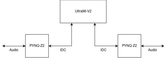
As stated before, we are going to connect the Ultra to multiple PYNQ boards for analog audio capabilities. To do this we will use a 22 pin ribbon cable (IDC).
What are the requirements?
For the Ultra expansion board we want the following requirements met:
- Ensure input protection for the delicate FPGA pins
- Provide a solid, and flexible way to connect multiple PYNQ-Z2 boards
- Expand all low speed header pins to a set usable 2.54mm pitch pinheaders
- Make sure the board is not specifically designed for this use case
- Ensure interoperability between the PYNQ-Z2 and Ultra
For the PYNQ expansion board we want the following requirements met:
- Make use of the Arduino header so that the PMOD and Raspberry headers are still usable
- Ensure interoperability between the PYNQ-Z2 and Ultra
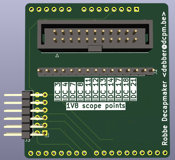
- Add scope point to be able to measure what's going on
We also want to be able to communicate at high speeds. For our particular case, we need 25MHz speeds, but higher speeds would be nice for the sake of making a generally usable board.
Revision A
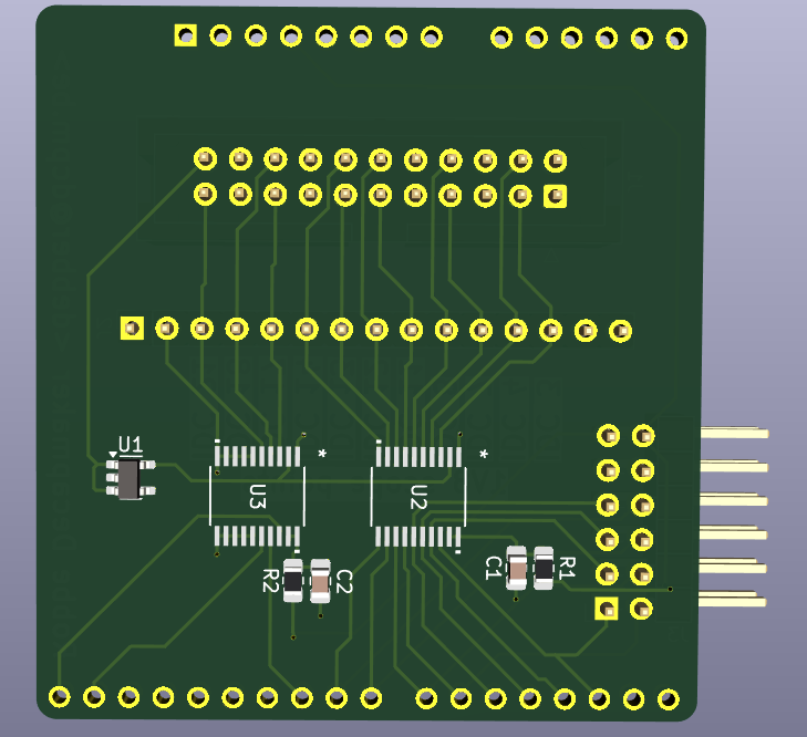
Ultra expansion board
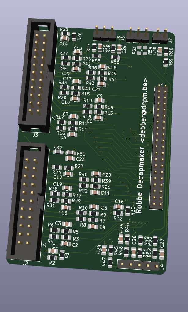
Some notes:
- Every unprotected FPGA input pin has an RCR T-filter (10 Ohm and 1nF)
- Every new output has a 2.54mm pitch for easy connections
- The IDC connectors have evenly divided I/O from the FPGA
- 5 general I/O
- 2 MIO
- 2 Ultra inputs (clk capable)
- I2C interface
- Extra I/O has been routed out to separate pinheaders
- SPI
- Extra MIO
- Power/Reset
- Power filtering on 5V using ferite beads
PYNQ expansion board
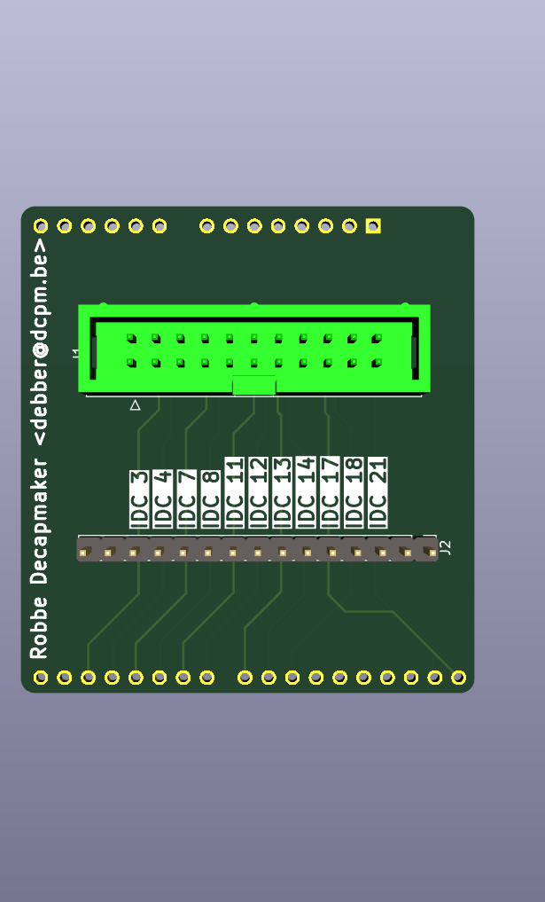
some notes:
- Very simple
- Added scope points between IDC and headers
Revision B
What went wrong with revA
When designing revision A, no thought was given to the voltage levels at which the FPGA I/O could run. Due to the layout of the respective boards, the Ultra and PYNQ have to use 1V8 and 3V3 I/O.
Solution
We decided to implement a fix on the PYNQ side of things because it is the simplest PCB to change. We implemented the following changes:
- Adding a PMOD connector for standalone operation without PYNQ board
- Adding bidirectional level shifters to fix the voltage level incompatibility
Results
When we tested revision A of the ultra PCB together with revision B of the PYNQ pcb for the first time, the results were less than stellar:
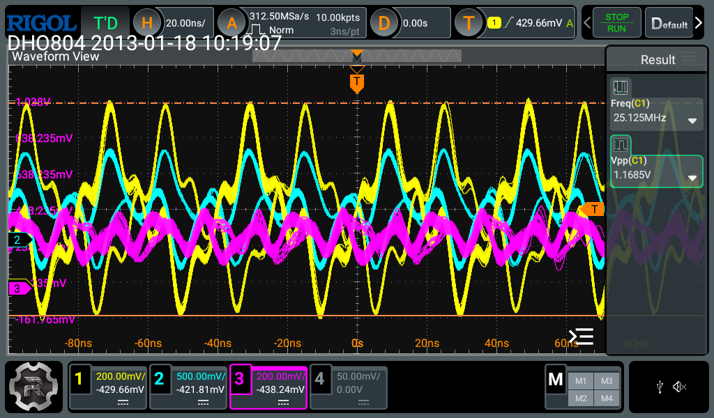
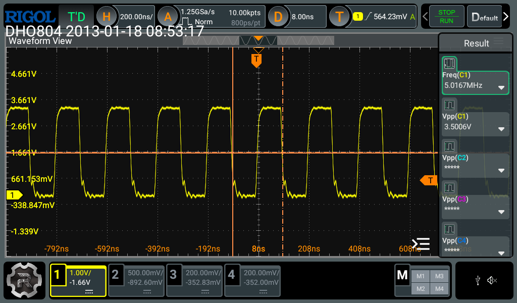
Here, the blue trace is the output of the PYNQ, the yellow trace is the signal after voltage translation from 3V3 to 1V8 and the pink line is what arrives at the ultra board. It does not take a lot of thought to realize this situation is less than ideal. We suspected that the design fell victim to improper signal integrity resulting in reflections. To combat this, we added a few temporary slew rate resistors before and after the level shifter in order to try to minimize the reflections. This gave us the following improvement:
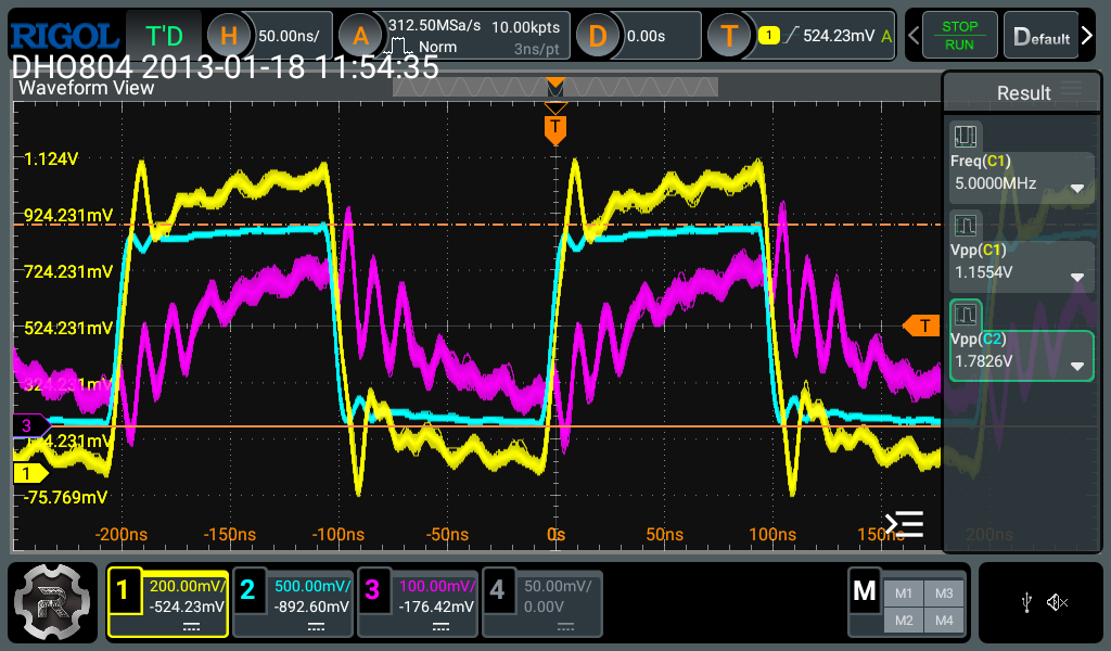
This is a nice improvement already, but there are still a lot of problems. Not the least of which is that the purple line still does not even come close to resembling a square wave. We also see that the square waves we get are still not ideal, they still contain ringing. Due to the large resistors we needed to get to this stage, they also did not have the right voltage anymore: 1V8 instead of 3V3 before down translation and 1V2 instead of 1V8 after down translation. We also decided to create a step input so that we could better see what was going on:
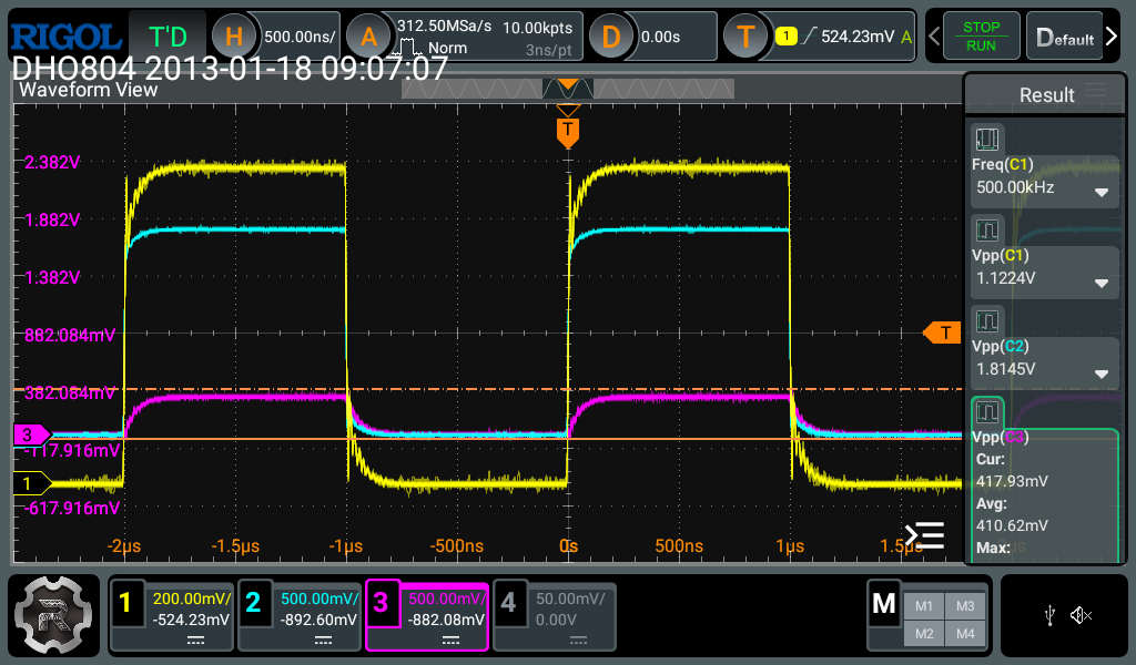
This more or less confirmed that we had major problems with very sharp edges. At this point, we needed some external help, a big thanks goes out to Gert Van Loock and Lode Decapmaker for taking the time to look at our problems and come up with a few tips which could help us fix these problems.
The 'solution' to these troubles
First and foremost, we removed all the temporary resistors and returned to the original design. Then we implemented the following suggestions:
-
We changed the pin configuration of the 7000 series to have a slow slewrate and minimal drive strength in order to reduce the sharp edges:
-
We made the filters on the Ultra board less harsh, this way they would interfere less with the signal
- Where needed on up translation (ultra to PYNQ), we can activate the
PULLUP trueconstraint on the PYNQ to address a missing pull up resistor on the PCB.
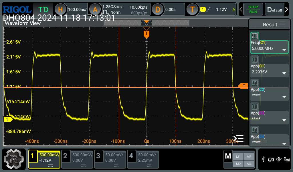
These changes gave us the following results:
- Output of the PYNQ (3V3)
- After voltage translation (1V8)
![]()
- At the ultra board:
Conclusion
The fixes suggested do certainly help, although it looks like there might still be a bit too much parasitic capacitance on the lines since the falling edge is not what we would expect. At the time of writing, we have also already invested in another commercial solution, so we might not make use of these PCBs at all.